Feedback Capacitor Low-Pass Filter Pitfalls

Feedback Capacitor Low-Pass Filter Pitfalls

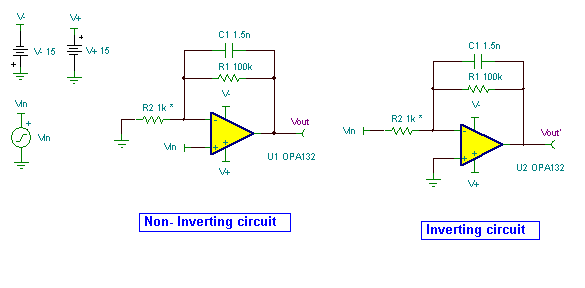
Adding a capacitor in parallel with the feedback resistor of an op amp is an easy way of accomplishing low- pass filtering. This technique works quite well in an inverting  amplifier (see the curves below) but not necessarily in a non-inverting amplifier. If the NI amplifier has high gain, the filtering is not bad– but inferior to the inverting case.  As the NI amplifier gain is reduced, the filter effectiveness suffers. In a gain of +2V/V, there is only 6dB of stopband attenuation. In a voltage-follower   (gain of +1V/V), there is no low- pass filtering at all! In each amplifier, the value of R2 was stepped logarithmically from 100 ohms to 100k.\e(x,2) (Circuit is created by Neil P. Albaugh, TI-Tucson )

Circuit for Demonstration of Pitfalls related with the Feedback Capacitor in Low-pass Filters 
Feedback Capacitor Low-Pass Filter Pitfalls
Demonstration of Pitfalls related with the Feedback Capacitor in Low-pass Filters circuits

The great feature of the TINA circuit simulator that you can analyze this circuit immediately with TINACloud the online version of TINA.

Click here to invoke TINACloud  and analyze the circuit yourself, or  watch our tutorial video to learn how to create and analyze this circuit with TINA off-line version now under Windows 10  or on-line with TINACloud.

You can send this link to any TINACloud customers and they can immediately load it by a single click and then run using TINACloud.

Download the FREE trial demo of TINA Design Suite and get

  1. One year free access to TINACloud (the cloud-based, multi-language, installation-free online version of TINA now running in your browser anywhere in the world.)
  2. An immediate 20% discount from the offline version of TINA
  3. Free license for your second computer, laptop etc.
Click here to download the FREE trial demo of TINA


Michael Koltai
www.tina.com

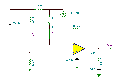
Creation and Simulation of a 1kV High Common Mode Voltage Difference Amplifier circuit with TINA or with TINACloud

High Common Mode Voltage Difference Amplifier circuit

Achieving a high common mode voltage differential amplifier requires a very high attenuation resistor network.

To minimize op amp input offset voltage and drift errors, an autozero type is used– OPA735.  An OPA335 can be used on a 5V supply. Common- mode rejection is critically dependent on the ratio matching of R3:R2 & R4:R1. These should be matched to extremely tight tolerances. Power dissipation in R3 & R4 are significant. Bypass capacitors are not shown.  (Circuit is created by Neil P. Albaugh  TI – Tucson)

High Common-Mode Voltage Difference Amplifier circuit:
1 kV High Common-Mode Voltage Difference Amplifier circuit
Creation and Simulation of a 1 kV High Common-Mode Voltage Difference Amplifier circuit

Watch our tutorial video to learn how to create and analyze this circuit with TINA off-line version  or on-line with TINACloud

Also if you download  the FREE trial demo of TINA Design Suite you can not only find and run this circuit but you will also get

    1. An immediate 20% discount from the offline version of TINA Design Suite
    2. Free license for your second computer, laptop etc.
    3. One year free access to TINACloud (the cloud-based, multi-language, installation-free online version of TINA now running in your browser anywhere in the world)

Click here  to download the FREE trial demo of TINA  Design Suite

Michael Koltai
www.tina.com