Instrumentation Amplifier Offset Correction Loop

Instrumentation Amplifier Offset Correction Loop

The feedback from integrator U2 provides a DC offset nulling function to the instrumentation amplifier (IA) U1. Although the IA response is similar to an AC- coupled amplifier, its input is, in fact, still DC- coupled and its input common-mode voltage limits must be observed.

Dc response can be preserved if a switch is added in series with R1. With the switch momentarily closed, the loop error is nulled and stored on C1 when the switch is open.
The switch converts the integrator into a sample/hold amplifier. To minimize correction voltage droop due to bias current, a JFET op amp such as an OPA132 is recommended for S/H use. Bypass capacitors are not shown. (Circuit is created by Neil P. Albaugh,  TI – Tucson)

Instrumentation Amplifier Offset Correction Loop circuit:
Instrumentation Amplifier Offset Correction Loop

Online Simulation of the Instrumentation Amplifier Offset Correction Loop Circuit

The great feature of the TINA circuit simulator that you can analyze this circuit immediately with TINACloud the online version of TINA. Of course you can also run this circuit in the off-line version of TINA.

Click here to invoke TINACloud  and analyze the circuit, or watch our tutorial video!

You can send this link to any TINACloud customers and they can immediately load it by a single click and then run using TINACloud.

Michael Koltai
www.tina.com

Fast Single-Supply Peak Detector

Fast Single-Supply Peak Detector

Notes:

1. Frequency compensation is determined by C1, C2, R2, and the sum of R1 and the forward resistance of D1. Since the dynamic resistance of D1 varies with current the peak detector must be analyzed for stability over its full output amplitude range.

2. The droop rate of the peak detector is determined by the input bias current of U1 plus the input bias current of the output buffer amplifier (not shown).

3. The input voltage range of 0 to +3.5V is limited by the CMV range of U1. R3 protects the op amp input from damage when the input voltage swings negative. (Circuit is created by Neil P. Albaugh  TI – Tucson)

Fast Single-Supply Peak Detector circuit:
Fast Single-Supply Peak Detector
Online Simulation of the Fast Single-Supply Peak Detector Circuit

The great feature of the TINA circuit simulator that you can analyze this circuit immediately with TINACloud the online version of TINA. Of course you can also run this circuit in the off-line version of TINA.

Click here to invoke TINACloud  and analyze the circuit, or watch our tutorial video! 

You can send this link to any TINACloud customers and they can immediately load it by a single click and then run using TINACloud.

Michael Koltai
www.tina.com

Single-Supply Bipolar Input Differential Output Amplifier

Single-Supply Bipolar Input Differential Output Amplifier

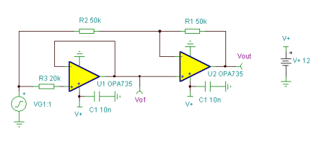
The rail- to- rail input and output characteristics of these CMOS op amps allow them to swing very close to their supply rails– +5V and ground.

By using both an inverting and noninverting amplifier output to swing only positive due to their not being capable of swinging below ground (0V). The op amps each act like a perfect rectifier.

Due to its unique R-R input topology, the OPA364 exhibits very high linearity over its entire common- mode input voltage range.

This absolute- value amplifier has a gain of 1V/V and has an input range of within a few mV of -5V to +5V. (Circuit is created by Neil P. Albaugh,  TI- Tucson)

Single-Supply Bipolar Input Differential Output Amplifier circuit:
Single- Supply Bipolar- Input Differential Output Amplifier
Single-Supply Bipolar Input Differential Output Amplifier
Online Simulation of the Single-Supply Bipolar Input Differential Output Amplifier Circuit

The great feature of the TINA circuit simulator that you can analyze this circuit immediately with TINACloud the online version of TINA. Of course you can also run this circuit in the off-line version of TINA.

Click here to invoke TINACloud  and analyze the circuit, or watch our tutorial video! 

You can send this link to any TINACloud customers and they can immediately load it by a single click and then run using TINACloud.

Michael Koltai
www.tina.com

Voltage-Controlled Electronic Load

Voltage-Controlled Electronic Load circuit:

This circuit is a voltage-controlled current sink.

It is scaled to provide a 500mA output current with a +1V input voltage.

This type of current sink can be very useful in power supply testing applications.

A R-R output op amp with an input common-mode range that includes its negative supply rail,  such as an OPA251, is required for single- supply operation.

Re- scaling this circuit with other Darlington transistors or low- threshold N-channel MOSFETs can result in an output current sink capability of many amps.

(Circuit is created by Neil P. Albaugh,  TI – Tucson)

Voltage-Controlled Electronic Load circuit:
Voltage-Controlled Electronic Load circuit
Online Simulation of the Voltage-Controlled Electronic Load Circuit

The great feature of the TINA circuit simulator that you can analyze this circuit immediately with TINACloud the online version of TINA. Of course you can also run this circuit in the off-line version of TINA.

Click here to invoke TINACloud  and analyze the circuit yourself, or watch our tutorial video! 

You can send this link to any TINACloud customers and they can immediatelly load it by a single click and then run using TINACloud.

Michael Koltai
www.tina.com

Differential Amplifier Resistor Tolerance Analysis

Differential Amplifier Resistor Tolerance Analysis

Make all resistors “Control Objects” and use “Parameter Stepping” to step each resistor value from 9.9k (1% low) to 10.1k (1% high) in 3 linear steps. Run DC Analysis, “DC Transfer Characteristic” and sweep “Vcmv” from -1V to +1V. The resulting family of curves shows the differential amplifier output error due to the various resistor tolerance combinations. The OPA277 error contribution is nil. Note that using 1% resistors in a differential amplifier design can result in a worst- case CMRR error of 20mV per volt of common-mode voltage. This is only 36dB! (Circuit is created Neil P. Albaugh  TI-Tucson)

Differential Amplifier Resistor Tolerance Analysis Circuit:
Differential Amplifier Resistor Tolerance Analysis Circuit


Online Simulation of the Differential Amplifier Resistor Tolerance Analysis Circuit

The great feature of the TINA circuit simulator that you can analyze this circuit immediately with TINACloud the online version of TINA. Of course you can also run this circuit in the off-line version of TINA.

Click here to invoke TINACloud  and analyze the circuit yourself, or watch our tutorial video! 

You can send this link to any TINACloud customers and they can immediatelly load it by a single click and then run using TINACloud.

Michael Koltai
www.tina.com