Universal Voltage Reference

Universal Voltage Reference
“This universal voltage reference circuit”- can provide a reference voltage that is continuously adjustable between -10V and +10V. If a REF02 is substituted for the  REF102 shown here, the output range will be -5V to +5V.The circuit uses both an op amp inverting gain path and a non- inverting  gain path simultaneously.  A potentiometer controls the ratio of these two gain paths. With the potentiometer wiper arm grounded,  U1 operates as an ordinary inverting amplifier with a gain of -1V/V. When the wiper arm is rotated to the other end of the potentiometer,  however, there is an additional gain path of +2V/V in addition to the -1V/V path. The resulting sum is a gain of +1V/V. At 50% rotation  (the wiper arm is exactly centered) the non- inverting gain path drops to +1V/V— cancelling the -1V/V gain entirely.  The output is then 0V. P1 should be a good quality potentiometer with high resolution and a good temperature coefficient.  Fortunately, the TC match of the resistance ratios of a potentiometer is much lower than its absolute resistance TC. (Circuit is created by Neil P. Albaugh  TI- Tucson)
Universal Voltage Reference
Universal Voltage Reference circuit
Online Simulation of the Universal Voltage Reference Circuit

The great feature of the TINA circuit simulator that you can analyze this circuit immediately with TINACloud the online version of TINA. Of course you can also run this circuit in the off-line version of TINA.

Click here to invoke TINACloud and analyze the circuit.

You can send this link to any TINACloud customers and they can immediatelly load it by a single click and then run using TINACloud.

Michael Koltai
www.tina.com

Differential Amplifier CMRR Trim Circuit

Online Simulation of the Differential Amplifier CMRR Trim Circuit

Adding a negative- resistance circuit (U2) to the REF pin allows the CMRR of a differential amplifier or instrumentation amplifier to be trimmed. This is done by applying a sine wave of 20Vp-p to the inputs of U1 and adjusting the potentiometer P1 for a minimum signal at the amplifier output.

By using an AC source the DC input offset errors do not effect this trim.

At 50% rotation of P1 the resistance of R8 cancels the resistance of R5, appearing as a virtual ground to the REF pin. As P1 is adjusted from end to end, R5 is “undercancelled”or “overcancelled” by R8 and the resistance presented to the REF pin goes from a real, positive resistance to a negative resistance. This allows the internal resistor network of U1to be trimmed for maximum CMRR. ( Circuit is created by Neil P. Albaugh  TI – Tucson )


Differential Amplifier CMRR Trim Circuit

Differential Amplifier CMRR Trim Circuit

Online Simulation of the Differential Amplifier CMRR Trim Circuit

The great feature of the TINA circuit simulator that you can analyze this circuit immediately with TINACloud the online version of TINA. Of course you can also run this circuit in the off-line version of TINA.

Click here to invoke TINACloud and analyze the circuit.

You can send this link to any TINACloud customers and they can immediatelly load it by a single click and then run using TINACloud.

Michael Koltai
www.tina.com
Cload Compensation

Cload Compensation

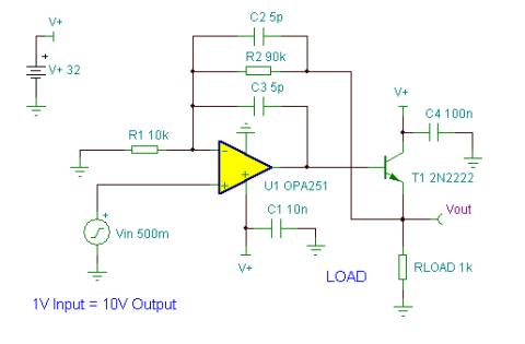
Driving a capacitive load directly with an op amp is an invitation to instability or oscillation. The amplifier’s output resistance and the load capacitance form a pole  in the feedback circuit. This inserts additional phase shift which will reduce the loop phase margin– perhaps to zero.

The effects of reduced phase margin can be  seen in the waveform ringing and gain peaking plots below. By isolating the capacitance with a small resistor (R1) and providing local high-frequency feedback (C2),  very little phase margin is lost. The voltage drop across R1 is sensed by a DC feedback connection (R2) to the circuit output and thereby reduced to virtually zero.
Note the improvement gained by compensating for a Cload!  (Circuit is created by Neil P. Albaugh,  TI – Tucson)

Cload Compensation  circuit:
Cload Compensation  circuit
Online Simulation of the Cload Compensation Circuit

The great feature of the TINA circuit simulator that you can analyze this circuit immediately with TINACloud the online version of TINA. Of course you can also run this circuit in the off-line version of TINA.

Click here to invoke TINACloud and analyze the circuit.

You can send this link to any TINACloud customers and they can immediatelly load it by a single click and then run using TINACloud.

Michael Koltai
www.tina.com
Grounded Cathode Laser Diode Driver

Grounded Cathode Laser Diode Driver

This circuit provides voltage- controlled constant-current biasing of a Grounded Cathode Laser Diode Driver by using a positive supply voltage and a positive control voltage.

As shown, the OPA569 op amp provides an output current of 500mA per volt input. Output is current- limited to 2A by R2. Frequency compensation is provided by C1 R1. This circuit takes advantage of the unique topology of the OPA569; it does not require a shunt resistor to measure its output current.

This amplifier provides an output monitor current from pin 19  that is 1/475 th of its output current.

The voltage drop across R2 due to this current is used as negative feedback to the amplifier’s inverting input (pin 5). Thus a constant- current output is derived by this feedback. Bypass capacitors are not shown.
Since no shunt resistor is required to measure output current, there is no reduction in output voltage compliance due to shunt resistor voltage drop and this circuit can swing its output voltage very close to its supply rail.

This increases efficiency and reduces heat sinking requirements. In fact, supply voltage can be reduced to 3.3V for most laser diodes.

The OPA569 features both a Current Limit (pin 4) and a Thermal Overtemp (pin 7) flag. These flags can be used to protect the amplifier and the Enable (pin 8) can be used to digitally control its status.

The “no connection” warnings simply indicate that these flags are not connected in this circuit; this does not affect the simulation.

(Circuit is created by Neil P. Albaugh,  TI – Tucson)

Online Simulation of the Grounded Cathode Laser Diode Driver Circuit

The great feature of the TINA circuit simulator that you can analyze this circuit immediately with TINACloud the online version of TINA. Of course you can also run this circuit in the off-line version of TINA.

Click here to invoke TINACloud and analyze the circuit.

You can send this link to any TINACloud customers and they can immediatelly load it by a single click and then run using TINACloud.

Michael Koltai
www.tina.com
Infrared Thermopile Detector Amplifier

Infrared Thermopile Detector Amplifier

This amplifier is designed for a thermopile infrared detector such as an S60M from Dexter Research. This detector output is 101mV/mW with a source resistance of 90k. A CMOS autozero OPA335 is used to minimize offset and drift as well as 1/f noise. The detector response time is 12ms so the amplifier frequency response  is rolled off to minimize its total output noise.
R3 & C2 add an additional pole to the amplifier’s rolloff; this improves the total output noise compared to the conventional R2 & C1 feedback filter. This improvement is evident in the noise plot below. U1 output is unipolar, so C2 can be a good tantalum capacitor.

The OPA335 output stage can be pulled- down to zero by an external  negative supply V-, even when operated on a single +5V power supply.

By not operating the op amp at the conventional “Vcc/2” bias point, the output is capable of full  rail- to- rail out-put, increasing the detector amplifier’s dynamic range. (Circuit created by Neil P. Albaugh,  TI – Tucson)

Infrared Thermopile Detector Amplifier
Online Simulation of the Infrared Thermopile Detector Amplifier Circuit

The great feature of the TINA circuit simulator that you can analyze this circuit immediately with TINACloud the online version of TINA. Of course you can also run this circuit in the off-line version of TINA.

Click the link below to invoke TINACloud and analyze the circuit.

https://www.tinacloud.com/tinademo/tina.php?c=54b3ae1ebcf37%3A415378

You can send this link to any TINACloud customers and they can immediatelly load it by a single click and then run using TINACloud.

Michael Koltai
www.tina.com