Creation and Simulation of a 1kV High Common Mode Voltage Difference Amplifier circuit with TINA or with TINACloud

High Common Mode Voltage Difference Amplifier circuit

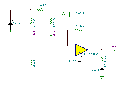
Achieving a high common mode voltage differential amplifier requires a very high attenuation resistor network.

To minimize op amp input offset voltage and drift errors, an autozero type is used– OPA735.  An OPA335 can be used on a 5V supply. Common- mode rejection is critically dependent on the ratio matching of R3:R2 & R4:R1. These should be matched to extremely tight tolerances. Power dissipation in R3 & R4 are significant. Bypass capacitors are not shown.  (Circuit is created by Neil P. Albaugh  TI – Tucson)

High Common-Mode Voltage Difference Amplifier circuit:
1 kV High Common-Mode Voltage Difference Amplifier circuit
Creation and Simulation of a 1 kV High Common-Mode Voltage Difference Amplifier circuit

Watch our tutorial video to learn how to create and analyze this circuit with TINA off-line version  or on-line with TINACloud

Also if you download  the FREE trial demo of TINA Design Suite you can not only find and run this circuit but you will also get

    1. An immediate 20% discount from the offline version of TINA Design Suite
    2. Free license for your second computer, laptop etc.
    3. One year free access to TINACloud (the cloud-based, multi-language, installation-free online version of TINA now running in your browser anywhere in the world)

Click here  to download the FREE trial demo of TINA  Design Suite

Michael Koltai
www.tina.com

Creation and Simulation of an OPA569 Laser Driver Circuit

Creation and Simulation of an OPA569 Laser Driver Circuit

The “OPA569 Laser Driver” circuit provides voltage- controlled constant- current biasing of a grounded- anode laser diode by using a negative supply voltage and a positive control voltage. As shown, the OPA569 op amp provides an output current of 500mA per volt input. Output is current- limited to 2A by R2. Frequency compensation is provided by C3 R3. This circuit takes advantage of the unique topology of the OPA569; it does not require a shunt resistor to measure its output current. This amplifier provides an output monitor current from pin 19 that is 1/475 th of its output current. This current is used as negative feedback to the amplifier’s inverting input (pin 5). A constant- current output is derived by this feedback.

Since no shunt resistor is required to measure output current, there is no reduction in output voltage compliance due to shunt resistor voltage drop and this circuit can swing its output voltage very close to its supply rail. This increases efficiency and reduces heat sinking requirements. In fact, supply voltage can be reduced to 3.3V for most laser diodes. The OPA569 features both a Current Limit (pin 4) and a Thermal Overtemp (pin 7) flag. These flags can be used to protect the amplifier and the Enable (pin 8) can be used to digitally control its status. (Circuit is created by Neil P. Albaugh, TI – Tucson)

OPA569 Laser Driver Circuit:

OPA569 Laser Driver for camtasia5

Creation and Simulation of an OPA569 Laser Driver Circuit

The great feature of the TINA circuit simulator that you can analyze this circuit immediately with TINACloud the online version of TINA.

Click here to invoke TINACloud  and analyze the circuit yourself, or  watch our tutorial video!

You can send this link to any TINACloud customers and they can immediatelly load it by a single click and then run using TINACloud.

Do you know that TINACloud also has an even more powerful downloadable offline version called TINA Design Suite?
TINA Design Suite is fully compatible with TINACloud and you can create, edit or run the same circuits in both systems. You can also easily exchange circuits between TINA Design Suite and TINACloud.

Download the FREE trial demo of TINA Design Suite and get

  1. One year free access to TINACloud (the cloud-based, multi-language, installation-free online version of TINA now running in your browser anywhere in the world.)
  2. An immediate 20% discount from the offline version of TINA
  3. Free license for your second computer, laptop etc.
Click here to download the FREE trial demo of TINA


Time to Voltage Converter

Time to Voltage Converter circuit

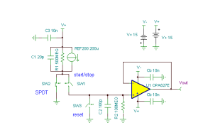
Applications such as rangefinders and ballistic chronographs require a high resolution measurement of time. This can be a time period of a few hundred nanoseconds to a few milliseconds. This is an analog circuit that can convert a time period to a voltage with high linearity and high resolution. In principle, a current source is used to charge a capacitor for the time interval and then the voltage across that capacitor is measured. A REF200 precision current source is used to furnish 200uA to a fast SPDT analog switch, represented by SW1 & SW2. This switch steers the current into ground or into a 100pF capacitor C2.

U1 is simply a high- precision buffer amplifier for the voltage on C2.

SW3 is a reset that zeros the voltage on C2. Initially, SW3 is open and SW2 steers the 200uA to ground until a START command is received; SW2 then opens and SW1 closes, steering the current into C2. The capacitor charges until a STOP command is received;  SW1 then opens and SW2 closes. The voltage on C2 is proportional to the time between START and STOP; scale time range is determined by the value of C2 so this capacitor should be high quality. A polystyrene or NPO (COG) ceramic is recommended for C2. A small DMOS SD211 can be used for SW3.  (Circuit is created by  Neil P. Albaugh, TI-Tucson)

Time to Voltage Converter circuit:
Time to Voltage Converter circuit


Online Simulation of a Time to Voltage Converter circuit:

The great feature of the TINA circuit simulator that you can analyze this circuit immediately with TINACloud the online version of TINA. Of course you can also run this circuit in the off-line version of TINA.

Click here to invoke TINACloud  and analyze the circuit yourself or watch our tutorial video!

You can send this link to any TINACloud customers and they can immediatelly load it by a single click and then run using TINACloud.

Michael Koltai
www.tina.com

Load Cancellation Circuit

Load Cancellation Circuit

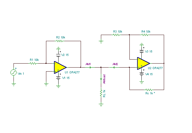
Amplifier output loading can be reduced or even eliminated by use of a load cancellation circuit such as that of U2. Without load cancellation, the inverting unity- gain op amp U1 output current is a function of its input voltage Vin and its 1k load resistance RL. At Vin = 1V, both AM1 (U1 output) and AMload (load current) = -1mA.

With compensation adjusted for 100%, the load current is furnished entirely by the compensation circuit. Thus the output of U1 essentially sees an “open circuit”. Rc controls the degree of load current compensation. Bypass capacitors are not shown. (Circuit is created by Neil P. Albaugh,  TI-Tucson)

Load Cancellation Circuit:
Load Cancellation Circuit


Online Simulation of a Load Cancellation Circuit:

The great feature of the TINA circuit simulator that you can analyze this circuit immediately with TINACloud the online version of TINA. Of course you can also run this circuit in the off-line version of TINA.

Click here to invoke TINACloud  and analyze the circuit yourself or watch our tutorial video!

You can send this link to any TINACloud customers and they can immediatelly load it by a single click and then run using TINACloud.

Michael Koltai
www.tina.com

Two OPA569 Current Sources in Parallel

Two OPA569 Current Sources in Parallel

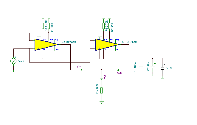
This circuit provides voltage- controlled constant- current biasing of a grounded- cathode laser diode. As shown, the OPA569 op amp provides an output current of 500mA per volt input. The OPA569’s output is current- limited to 2A by R3 & R4. Bypass capacitors are not shown. This circuit takes advantage of the unique topology of the OPA569; it does not require a shunt resistor to measure its output current. This amplifier provides an output monitor current from pin 19  that is 1/475 th of its output current. The voltage developed across R1 & R2 are used as negative feedback to the amplifier’s inverting input (pin 5).

A constant- current output is derived by this feedback.

Since no shunt resistor is required to measure output current, there is no reduction in output  voltage compliance due to shunt resistor voltage drop, this circuit can swing its output voltage very close to its supply rail. This increases efficiency and reduces heat sinking requirements. In fact, supply voltage can be reduced to only a few hundred mV above the load voltage.
The OPA569 features both a Current Limit (pin 4) and a Thermal Overtemp (pin 7) flag. These flags can be used to protect the amplifier and the Enable (pin 8) can be used to digitally control its status. (Circuit is created by  Neil P. Albaugh,  TI-Tucson)

Two OPA569 Current Sources in Parallel Circuit:
Two OPA569 Current Sources in Parallel
Online Simulation of the “Two OPA569 Current Sources in Parallel” Circuit:

The great feature of the TINA circuit simulator that you can analyze this circuit immediately with TINACloud the online version of TINA. Of course you can also run this circuit in the off-line version of TINA.

Click here to invoke TINACloud and analyze the circuit yourself or watch our tutorial video!

You can send this link to any TINACloud customers and they can immediatelly load it by a single click and then run using TINACloud.

Michael Koltai
www.tina.com