Shunt Amplifier with Offset Output

Shunt Amplifier with Offset Output

By reducing the +12V common- mode voltage, an INA122 can sense the voltage drop across a shunt resistor while being powered by the same +12V power supply.  Rg controls the voltage gain of U1. This circuit is scaled for a 2.5V output range centered around +1.25V; thus this amplifier can measure bidirectional shunt current. An INA122 does not feature a R-R output so the sinking current is limited to about -0.3A. This can be useful where battery current must be monitored while it is being charged or discharged. Bypass capacitors are not shown. (Circuit is created by Tucson)

Shunt Amplifier with Offset Output circuit:
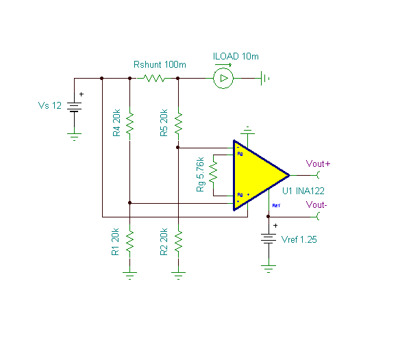
Shunt amplifier with offset output
Online Simulation of a Shunt Amplifier with Offset Output Circuit:

The great feature of the TINA circuit simulator that you can analyze this circuit immediately with TINACloud the online version of TINA. Of course you can also run this circuit in the off-line version of TINA.

Click here to invoke TINACloud and analyze the circuit yourself or watch our tutorial video!

You can send this link to any TINACloud customers and they can immediatelly load it by a single click and then run using TINACloud.

Michael Koltai
www.tina.com

Single-Ended Input Differential Output Amplifier

Single-Ended Input Differential Output Amplifier

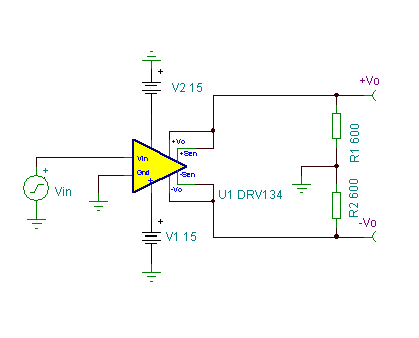
A DRV134 converts a single- ended input signal to a differential output. Differential output is used to drive the inputs of some A/D converters and to drive tristed- pair or Twinax transmission lines in a high- noise environment.

An INA137 or INA137 can be used as a differential line receiver to convert the differential voltage back to single- ended.

In AC- only applications such as audio, capacitors can be inserted between the outputs and their respective sense pins to reduce the DRV134 output DC offset. See the data sheet for details. Bypass capacitors have been omitted in this schematic but their use is recommended. (Circuit is created by Neil P. Albaugh, TI- Tucson )

Single-Ended Input Differential Output Amplifier  Circuit:
Single-Ended Input Differential Output Amplifier
Online Simulation of a Single-Ended Input Differential Output Amplifier  Circuit

The great feature of the TINA circuit simulator that you can analyze this circuit immediately with TINACloud the online version of TINA. Of course you can also run this circuit in the off-line version of TINA.

Click here to invoke TINACloud and analyze the circuit yourself or watch our tutorial video!

You can send this link to any TINACloud customers and they can immediatelly load it by a single click and then run using TINACloud.

Michael Koltai
www.tina.com
PI Temperature Control Integrator

PI Temperature Control Integrator
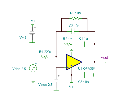
Proportional-integral response for control systems can be generated by a simple analog circuit. Feedback components R2, C2, & C1 together with input resistor R1 control the frequency response of U1. R3 is added to the circuit to provide feedback in a DC analysis and it is not necessary in an actual circuit. For stability, the control loop dominant pole should be formed by this integrator. (Circuit is created by Neil P. Albaugh, TI-Tucson)

PI Temperature Control Integrator circuit:
PI Temperature Control Integrator circuit
Online Simulation of a PI Temperature Control Integrator Circuit

The great feature of the TINA circuit simulator that you can analyze this circuit immediately with TINACloud the online version of TINA. Of course you can also run this circuit in the off-line version of TINA.

Click here to invoke TINACloud and analyze the circuit, or watch our tutorial video!

You can send this link to any TINACloud customers and they can immediatelly load it by a single click and then run using TINACloud.

Michael Koltai
www.tina.com
Very Low DC Offset Wideband Amplifier

Very Low DC Offset Wideband Amplifier

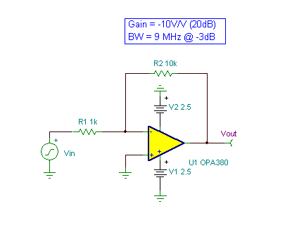
The OPA380 is an integrator-stabilized operational amplifier that was developed primarily for transimpedance amplifier applications. Its inverting input is that a 90MHz CMOS op amp but its non-inverting input is an integrator non-inverting input, allowing only very low frequency response through this input. In most dual- supply applications, the OPA380 non- inverting input is simply tied to ground. In single- supply applications, it can be used to provide a DC offset. By adding an input resistor, R1, a transimpedance amplifier is transformed into a conventional inverting amplifier. The usual op amp inverting gain equation  applies: Av = – (R2/R1) in V/V. The OPA380 is input offset voltage is specified as 4uV typical, 25uV maximum @ 25C, drift is 0.03uV/C typ, 0.1uV/C max.  (Circuit is created by Neil P. Albaugh  TI- Tucson)

 Very Low DC Offset Wideband Amplifier circuit:
Very Low DC Offset Wideband Amplifier
Online Simulation of the Very Low DC Offset Wideband Amplifier Circuit

The great feature of the TINA circuit simulator that you can analyze this circuit immediately with TINACloud the online version of TINA. Of course you can also run this circuit in the off-line version of TINA.

Click here to invoke TINACloud and analyze the circuit, or watch our tutorial video!

You can send this link to any TINACloud customers and they can immediatelly load it by a single click and then run using TINACloud.

Michael Koltai
www.tina.com
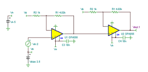
Wideband 75MHz 28dB Gain Amplifier

Wideband 75MHz 28dB Gain Amplifier

This Wideband 75MHz 28dB Gain Amplifier circuit is based on two OPA355 gain stages in cascade. The dual version, OPA2355, can also be used. An OPA355 achieves low input bias current, +/-50pA MAZ, low voltage noise, 5.8nV/sq-rt Hz typical @ 1MHz, and it has good gain-bandwidth, 200MHz, and high slew rate, 300V/us. To maximize bandwidth in a 2-stage amplifier, each stage should be set to a gain of the square- root of the total cascaded amplifier gain. A triple op amp, OPA3355 can be cascaded to provide even higher BW at the same gain. (Created by Neil P. Albaugh  TI- Tucson)

Wideband amplifier circuit:
Wideband 75MHz 28dB Gain Amplifier
Online Simulation of the “Wideband 75MHz 28dB Gain Amplifier” Circuit

The great feature of the TINA circuit simulator that you can analyze this circuit immediately with TINACloud the online version of TINA. Of course you can also run this circuit in the off-line version of TINA.

Click here to invoke TINACloud and analyze the circuit, or watch our tutorial video!

You can send this link to any TINACloud customers and they can immediatelly load it by a single click and then run using TINACloud.

Michael Koltai
www.tina.com