Capacitance Bridge

Capacitance Bridge

This circuit below is a capacitance bridge; it detects the matching between a reference capacitance C1 and an unknown capacitance, Cx. It uses an instrumentation amplifier in an unusual topology– a sine wave drives the two input op amps’ non- inverting inputs (ordinarily the IA inputs) and the internal 25k feedback resistor of each op amp forces that sine wave to appear at the op amp’s inverting inputs (ordinarily the IA gain resistor connections). The impressed AC voltage across each capacitor causes current to flow in each feedback resistor and this creates a voltage at the output of each of the two input op amps. The third IA stage, a differential amplifier, subtracts the two voltages. Thus, when Cx = C1, the output voltage is zero.

A higher or lower capacitance at Cx unbalances the bridge

and an output results that is proportional to the capacitance difference; a high/low mismatch is indicated by a 180 degree phase difference.

A synchronous detector (aka phase- sensitive demodulator) driven by F and low- pass filtered will result in a capacitance bridge DC output that is at null when Cx = C1.  The sensitivity of the bridge is proportional to F, both in amplitude and frequency, and to the reference capacitance C1. Higher frequencies result in higher output voltages but the inevitable IA CMRR roll- off at high frequencies will reduce the depth of the null voltage.  An advantage of this circuit is that it is quite simple and it allows both capacitors to be ground- referenced.  (Circuit is created by Neil P. Albaugh,  TI-Tucson)

Capacitance Bridge circuit:

Capacitance Bridge-blog

Online Simulation of the “Capacitance Bridge” Circuit

The great feature of the TINA circuit simulator that you can analyze this circuit immediately with TINACloud the online version of TINA. Of course you can also run this circuit in the off-line version of TINA.

Click here to invoke TINACloud and analyze the circuit, or watch our tutorial video!

You can send this link to any TINACloud customers and they can immediatelly load it by a single click and then run using TINACloud.

Michael Koltai
www.tina.com

Triangle & Square Wave Oscillator 1kHz

Triangle & Square Wave Oscillator 1kHz

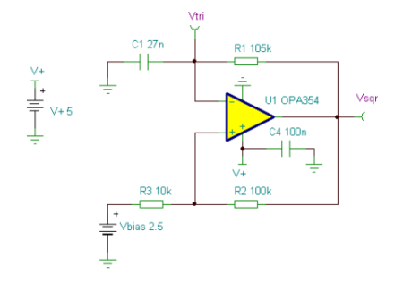
This simple relaxation oscillator provides both a square- wave and a triangular- wave output. This oscillator is biased for operation on a single +5V supply. The DC component of each output can be removed by capacitive coupling if necessary.Since a rail-to-rail output op amp is used for U1, the square wave output amplitude is the same as its supply voltage. A lower quiescent current op amp such as an OPA364 can be used if Iq is important. Oscillator frequency is determined by C1 & R1. The Transient Analysis used the “Zero initial conditions” to aid the oscillator start- up. This start- up time is visible for the first few milliseconds in the waveform above. (Circuit is created by Neil P. Albaugh  TI- Tucson)


“Triangle & Square Wave Oscillator 1kHz” circuit:
Triangle & Square Wave Oscillator 1kHz
Online Simulation of the “Triangle & Square Wave Oscillator 1kHz” Circuit

The great feature of the TINA circuit simulator that you can analyze this circuit immediately with TINACloud the online version of TINA. Of course you can also run this circuit in the off-line version of TINA.

Click here to invoke TINACloud and analyze the circuit, or watch our tutorial video!

You can send this link to any TINACloud customers and they can immediatelly load it by a single click and then run using TINACloud.

Michael Koltai
www.tina.com

Programmable-Brightness LED Control

Programmable-Brightness LED Control

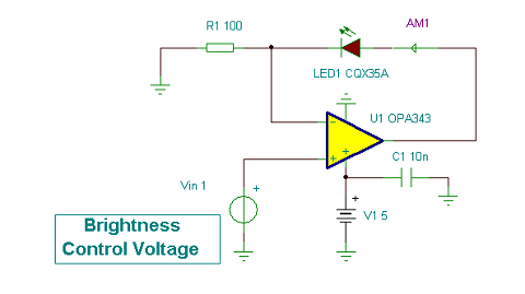
This simple op amp circuit can be used to control the brightness of a LED. By placing the LED in the op amp feedback, it is driven  in a constant- current mode. This eliminates the diode forward voltage temperature coefficient’s effect on its current and thus its  brightness over temperature.  This circuit is a voltage- controlled current source. (Circuit is created by Neil P. Albaugh,  TI – Tucson)

Programmable-Brightness LED Control circuit:
Programmabe-brightness LED control
Programmable-Brightness LED Control circuit
Online Simulation of the Programmable-Brightness LED Control Circuit

The great feature of the TINA circuit simulator that you can analyze this circuit immediately with TINACloud the online version of TINA. Of course you can also run this circuit in the off-line version of TINA.

Click here to invoke TINACloud  and analyze the circuit, or watch our tutorial video!

You can send this link to any TINACloud customers and they can immediatelly load it by a single click and then run using TINACloud.

Michael Koltai
www.tina.com
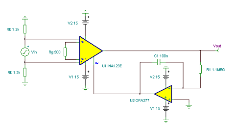
Instrumentation Amplifier Offset Correction Loop

Instrumentation Amplifier Offset Correction Loop

The feedback from integrator U2 provides a DC offset nulling function to the instrumentation amplifier (IA) U1. Although the IA response is similar to an AC- coupled amplifier, its input is, in fact, still DC- coupled and its input common-mode voltage limits must be observed.

Dc response can be preserved if a switch is added in series with R1. With the switch momentarily closed, the loop error is nulled and stored on C1 when the switch is open.
The switch converts the integrator into a sample/hold amplifier. To minimize correction voltage droop due to bias current, a JFET op amp such as an OPA132 is recommended for S/H use. Bypass capacitors are not shown. (Circuit is created by Neil P. Albaugh,  TI – Tucson)

Instrumentation Amplifier Offset Correction Loop circuit:
Instrumentation Amplifier Offset Correction Loop

Online Simulation of the Instrumentation Amplifier Offset Correction Loop Circuit

The great feature of the TINA circuit simulator that you can analyze this circuit immediately with TINACloud the online version of TINA. Of course you can also run this circuit in the off-line version of TINA.

Click here to invoke TINACloud  and analyze the circuit, or watch our tutorial video!

You can send this link to any TINACloud customers and they can immediately load it by a single click and then run using TINACloud.

Michael Koltai
www.tina.com
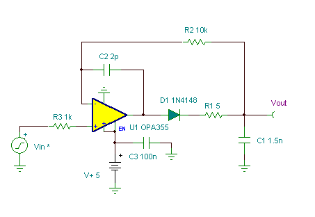
Fast Single-Supply Peak Detector

Fast Single-Supply Peak Detector

Notes:

1. Frequency compensation is determined by C1, C2, R2, and the sum of R1 and the forward resistance of D1. Since the dynamic resistance of D1 varies with current the peak detector must be analyzed for stability over its full output amplitude range.

2. The droop rate of the peak detector is determined by the input bias current of U1 plus the input bias current of the output buffer amplifier (not shown).

3. The input voltage range of 0 to +3.5V is limited by the CMV range of U1. R3 protects the op amp input from damage when the input voltage swings negative. (Circuit is created by Neil P. Albaugh  TI – Tucson)

Fast Single-Supply Peak Detector circuit:
Fast Single-Supply Peak Detector
Online Simulation of the Fast Single-Supply Peak Detector Circuit

The great feature of the TINA circuit simulator that you can analyze this circuit immediately with TINACloud the online version of TINA. Of course you can also run this circuit in the off-line version of TINA.

Click here to invoke TINACloud  and analyze the circuit, or watch our tutorial video! 

You can send this link to any TINACloud customers and they can immediately load it by a single click and then run using TINACloud.

Michael Koltai
www.tina.com