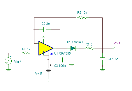
Fast Single-Supply Peak Detector
Notes:
1. Frequency compensation is determined by C1, C2, R2, and the sum of R1 and the forward resistance of D1. Since the dynamic resistance of D1 varies with current the peak detector must be analyzed for stability over its full output amplitude range.
2. The droop rate of the peak detector is determined by the input bias current of U1 plus the input bias current of the output buffer amplifier (not shown).
3. The input voltage range of 0 to +3.5V is limited by the CMV range of U1. R3 protects the op amp input from damage when the input voltage swings negative. (Circuit is created by Neil P. Albaugh TI – Tucson)
Fast Single-Supply Peak Detector circuit:

Online Simulation of the Fast Single-Supply Peak Detector Circuit
The great feature of the TINA circuit simulator that you can analyze this circuit immediately with TINACloud the online version of TINA. Of course you can also run this circuit in the off-line version of TINA.
Click here to invoke TINACloud and analyze the circuit, or watch our tutorial video!
You can send this link to any TINACloud customers and they can immediately load it by a single click and then run using TINACloud.
Michael Koltai
www.tina.com
