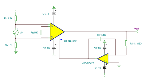
Instrumentation Amplifier Offset Correction Loop
The feedback from integrator U2 provides a DC offset nulling function to the instrumentation amplifier (IA) U1. Although the IA response is similar to an AC- coupled amplifier, its input is, in fact, still DC- coupled and its input common-mode voltage limits must be observed.
Dc response can be preserved if a switch is added in series with R1. With the switch momentarily closed, the loop error is nulled and stored on C1 when the switch is open.
The switch converts the integrator into a sample/hold amplifier. To minimize correction voltage droop due to bias current, a JFET op amp such as an OPA132 is recommended for S/H use. Bypass capacitors are not shown. (Circuit is created by Neil P. Albaugh, TI – Tucson)
Instrumentation Amplifier Offset Correction Loop circuit:

Online Simulation of the Instrumentation Amplifier Offset Correction Loop Circuit
The great feature of the TINA circuit simulator that you can analyze this circuit immediately with TINACloud the online version of TINA. Of course you can also run this circuit in the off-line version of TINA.
Click here to invoke TINACloud and analyze the circuit, or watch our tutorial video!
You can send this link to any TINACloud customers and they can immediately load it by a single click and then run using TINACloud.
Michael Koltai
www.tina.com
